Soutenance de thèse – Baptiste Robbiani – Mardi 16 décembre 2025 à 09h45 – amphi Concorde U4 UT
Baptiste Robbiani soutiendra sa thèse le mardi 16 décembre 2025 à 09h45 – amphi Concorde U4 à l’UT, sur le sujet : « Analyse de
Baptiste Robbiani soutiendra sa thèse le mardi 16 décembre 2025 à 09h45 – amphi Concorde U4 à l’UT, sur le sujet : « Analyse de
Sariette NOWA soutiendra sa thèse le vendredi 26 septembre 2025 à 9h30, lieu de soutenance : 325-327 118 Rte de Narbonne, bat 3R1 B4 31400
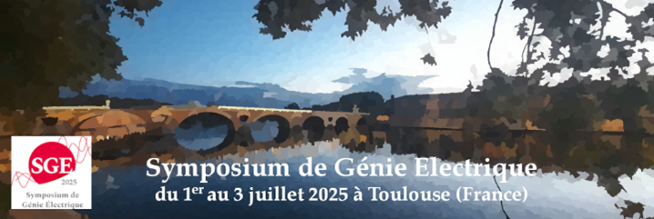
Le 6ème symposium de génie électrique, SGE2025, a eu lieu à Toulouse du 1er au 3 Juillet, au centre de congrès Pierre Baudis. Ce symposium,
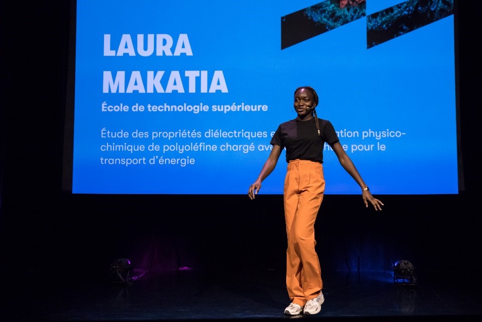
Laura Makatia : Lauréate de l’édition MT180 2025 de l’Ecole Supérieure de Technologie de Montréal
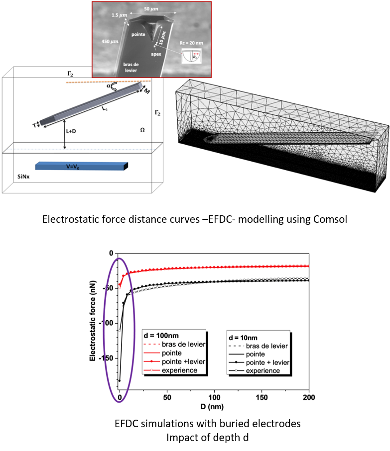
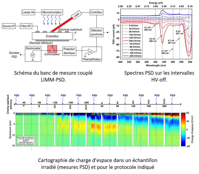
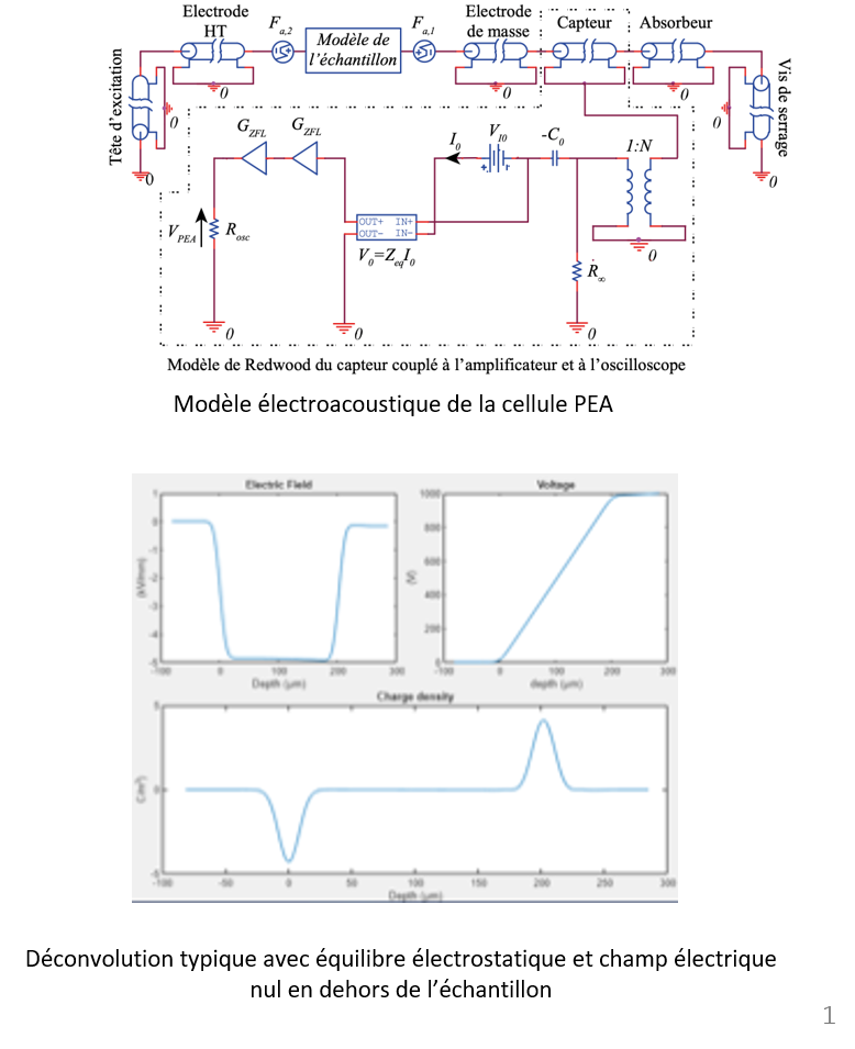
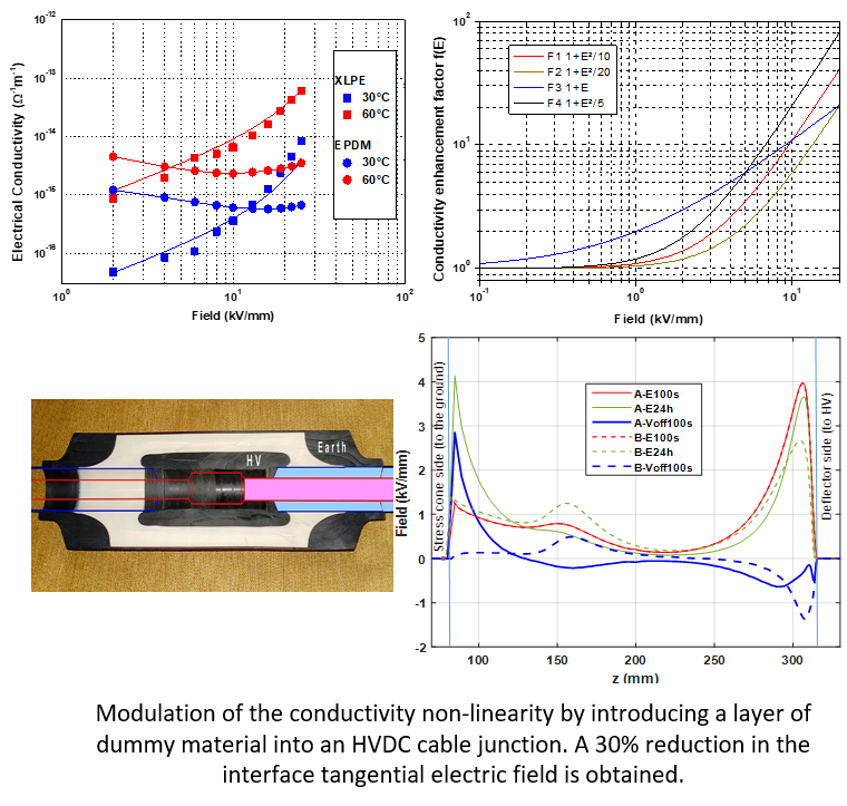
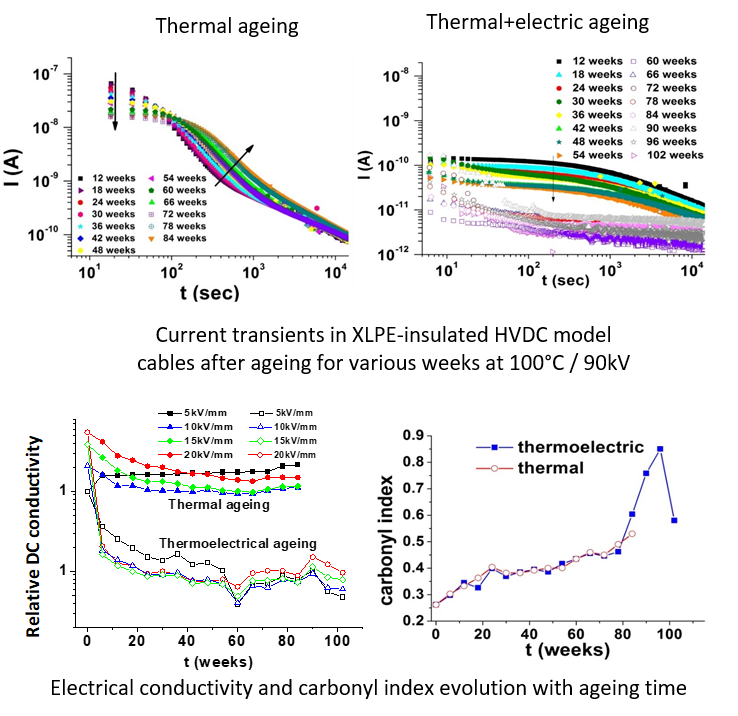
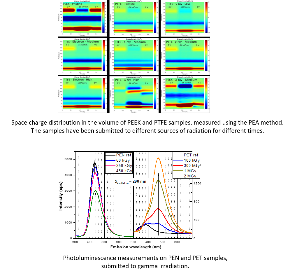
La soutenance de thèse d’Assane NDOUR intitulée : “Modélisation et caractérisation expérimentale du champ électrique et des charges dans un isolant de câbles HVDC de
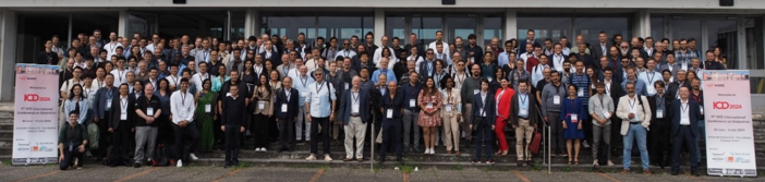
La 5e International Conference in Dielectrics (ICD) s’est tenue à Toulouse du 30 juin au 5 juillet 2024 sur le site de l’Université Toulouse III
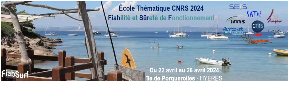
Après Oléron en 2019 et Cahors en 2022, la troisième édition de l’école thématique FiabSurf s’est tenue du 22 au 26 avril 2024 sur l’île

11 chercheurs et enseignant-chercheurs du LAPLACE référencés dans le “TOP 2% Scientists Worldwide” d’après l’étude Standford s’appuyant sur l’impact des travaux des
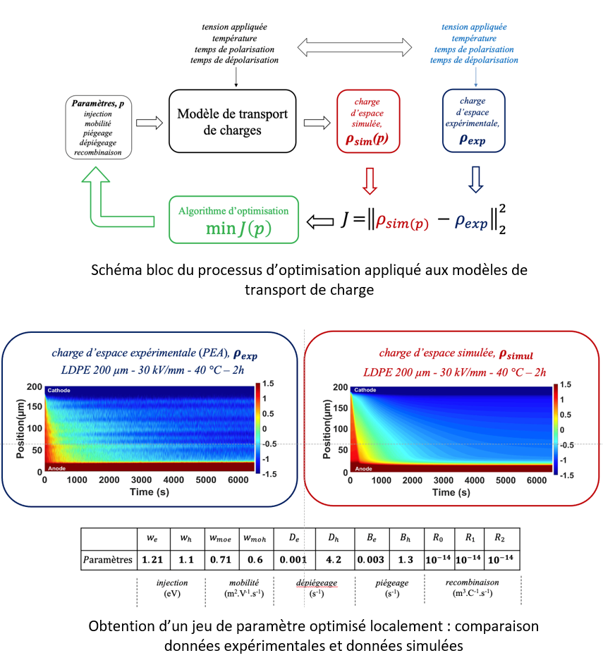
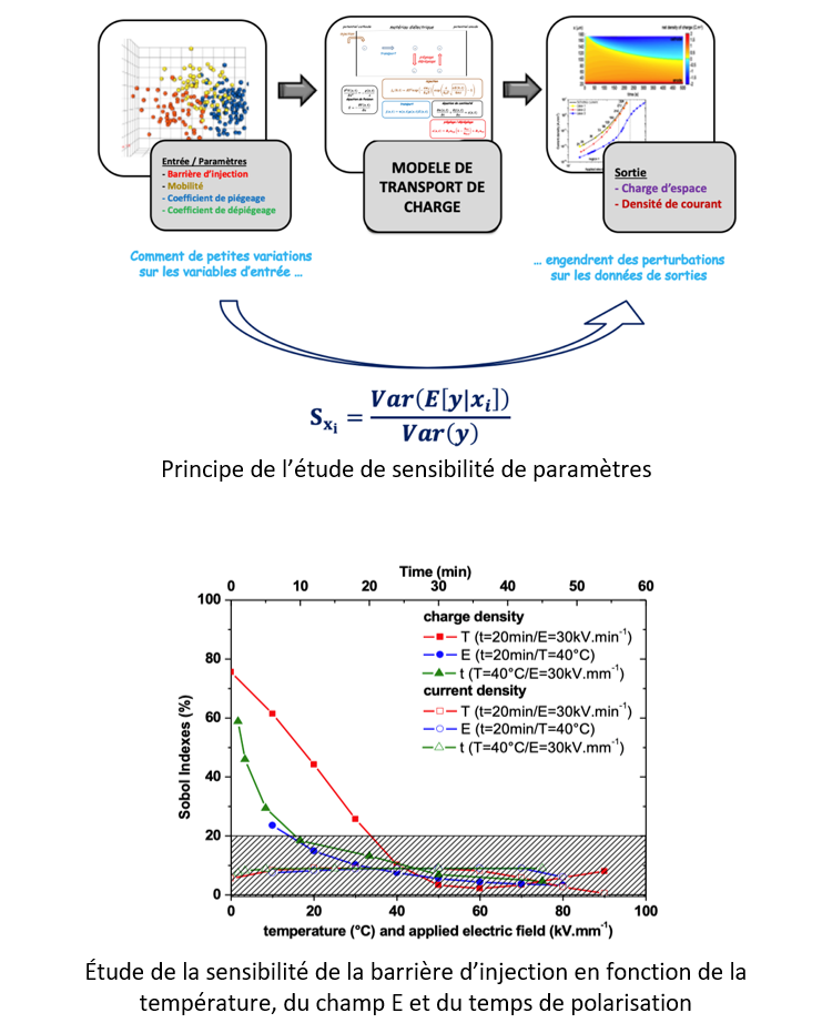
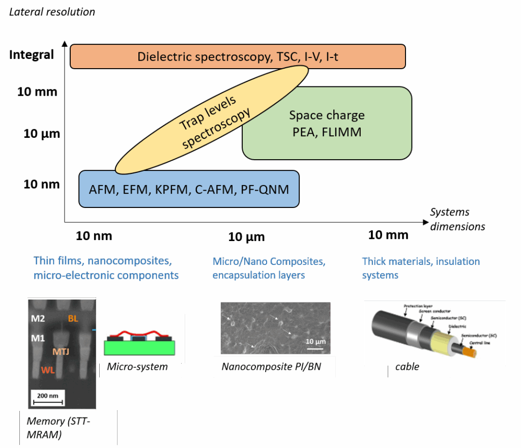
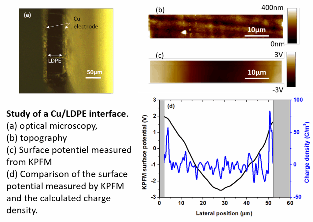
La soutenance de thèse de Duvan MENDOZA-LOPEZ , intitulée “Étude des phénomènes de piégeage et dépiégeage de charges par mesures de charge d’espace et de
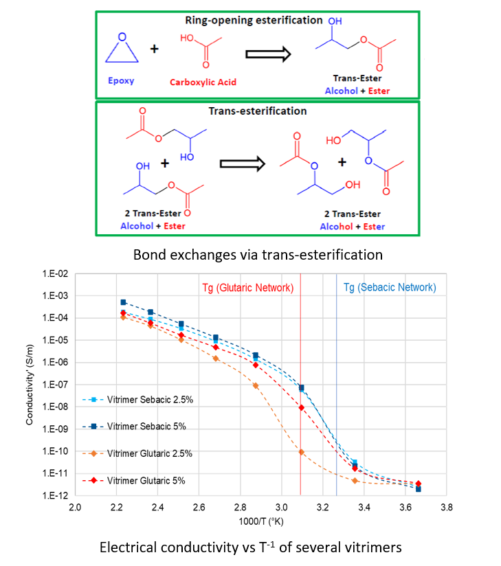
La soutenance de thèse de Baptiste ARATI, intitulée “Manufacturing and characterization of self-healing polymers intended for the electrical insulation of future power modules”, aura lieu