Soutenance de thèse – Luc BIMMEL – Vendredi 20 février à 09 h 00 – Salle des thèses C002, ENSEEIHT
Luc BIMMEL soutiendra sa thèse le vendredi 20 février 2026 à 09 h 00 en salle des thèses de l’ENSEEIHT (Amphi C002), au 2 Rue
The group’s activities and areas of application are presented in the figure below. :
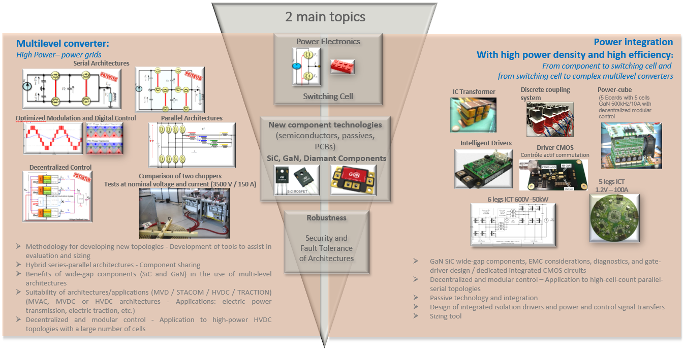
These two cross-cutting themes led us to structure our team according to 4 research operations :
OP1 : High-power architectures, energy network applications and digital control of complex hybrid structures
OP2 : Study methods and tools for the design of power converters
OP3 : Architectures and technologies for power integration
OP4 : Architectures and technologies adapted for integrated electrical safety and availability
Our research activities address the main challenges of electrical energy conversion and are based on a combination of theoretical and experimental approaches centered around the concept of the switching cell.
The group has specialized in the study of new multicellular converter structures for medium and high power applications (from kW to MW), involving original arrangements of switching cells: series-nested, parallel-stacked, and global or partial parallelization through innovative magnetic coupling devices. These arrangements, whether used individually or combined, are designed to produce high-frequency, multilevel waveforms that significantly reduce filtering costs across a wide range of applications :
This by integrating the constraints specific to these areas from the design phase.
The validation of these new converter structures requires the specific development of fast analog and digital control systems, enabling the observation and management of all internal state variables. This validation process systematically involves the experimental implementation at a significant power level, which requires addressing challenges related to connectivity, thermal management, three-dimensional assembly, and the integration of control systems (ASIC, FPGA, HIL). Simulation, co-simulation, and optimization tools are used, adapted, and coupled to globally determine the best trade-offs during the design and close-loop control phases (PWM).
These studies are complemented by research on the robustness of power components and their failure modes in relation to circuit topology, leading to the development of new secure and fault-tolerant structures.
The scientific objectives pursued by the Static Converters group (CS) focus on advancing research in power electronics, contributing to the development and acquisition of new knowledge in the field, and promoting its transfer through industrial partnerships addressing major societal challenges in the field of electrical energy management (efficiency, conversion, integration, reliability, etc.).
The team’s strategy is structured in two main stages: the first involves developing, studying, or improving new technologies, topologies, and methods through the use of internal resources or public funding. This stage aims to drive innovation and advance the frontiers of knowledge in our field. The second stage focuses on technology transfer and value creation through industrial partnerships, either directly through contractual collaborations or via national or international projects. This second stage can also foster close collaborations with industrial partners and may even lead to the creation of startups.
Anne Castelan, Didier Flumian and Nicolas Rouger – High-power electronic transformer based on SiC components :

Yuying Shi, Maxime Pain and Thierry Meynard – Validation of inter-cell transformer sizing procedures :

The research carried out in this area mainly focuses on the development and design of multicellular converters, aiming to optimize energy efficiency and waveform quality through the combination of elementary switching cells or converter assemblies. Multicellular topologies improve converter performance, though at the cost of greater complexity, involving more semiconductors and the addition of passive components (capacitors) within the switching cell.
Regarding our recent work:
For medium-voltage applications in three-phase structures, some components can be shared across phases. This innovative principle has been applied in the following cases:
In the study of a Common Flying Capacitor (CFC) topology, where switching cells and flying capacitors are shared between the three phases of a three-phase inverter. This sharing reduces the number of components and increases the power density of the converter, while maintaining the advantages of multilevel topologies—an essential factor for the electrification of air and ground transportation.
In the development of a medium-voltage three-phase inverter topology, where switching stress is concentrated within a shared leg, enabling the design of 4.16 kV and 6.6 kV motor drives by combining 1.7 kV components (switching at several kHz) with 4.5 kV or 6.5 kV components (operating at 50 Hz to route the power flow).
Thus, the use of low-voltage components improves efficiency and significantly reduces costs. However, these new topologies, despite effectively reducing stored energy and the number of active components, present control and regulation challenges, especially in maintaining constant flying capacitor voltages. Tailored control strategies have been developed, such as decentralized/distributed control of multicellular converters, which is currently being applied in a dedicated European project (Horizon-Europe SCOPS).
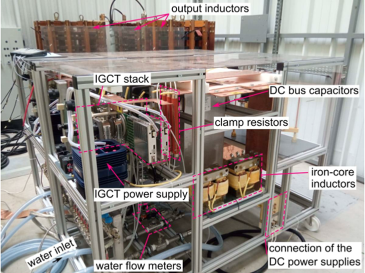
In AC/DC converter stations for HVDC grids, the Modular Multilevel Converter (MMC) topology is now widely used. In the GW power range, selecting the right semiconductor components for the elementary cell is critical to maximizing efficiency. Our work has demonstrated the relevance of IGCTs (Integrated Gate-Commutated Thyristors) for this type of application, challenging the industry’s widespread preference for IGBTs. An electro-thermal model was developed in our laboratory to accurately predict losses and junction temperatures in each semiconductor of an MMC arm.
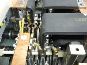
Following this study, a continuous-operation test bench, composed of two opposing IGCT-based cells, was designed and implemented to validate the electro-thermal model. With a DC bus voltage up to 5 kV and currents exceeding 2 kA, 4.5 kV and 10 kV components were tested under operating conditions equivalent to those of a 1 GW converter station.

High-power electronic transformer based on SiC components :

Power wiring in the opposition bench of two IGCT cells – Produced by Jean-Marc Blaquière :
Multicellular converter architectures are a recognized specialty of our team; they have led to several successful technology transfers to industry, initially in the Medium Voltage and High Power range (1–10 kV, 1–10 MW) and have gradually expanded into lower voltage and power domains, with the most recent applications in the internal power supplies of mobile phones (1–5 V, 1–10 W).
In parallel, the revolution in wide bandgap power semiconductor components has significantly impacted our field, opening new possibilities for system improvements.
Between series, parallel, and hybrid architectures – allowing the combination of components with different voltage and current ratings – and the choice between conventional silicon (Si) components and wide bandgap devices, designers now have an increased number of degrees of freedom. However, no universal hierarchy exists in this field. Specific methods and tools must therefore be developed to assist in designing the next generation of converters.
Our team has always paid great attention to clearly describing the fundamental principles governing our discipline (as demonstrated by our contributions to the ‘Techniques de l’Ingénieur’), and this approach has ultimately driven our recent and ongoing research into design and analysis methods.
The development of a unified formalism, which treats classical power electronics as a particular case of multicellular converters, has allowed us to create generic models capable of quickly comparing solutions based on different technologies (Si, SiC, or GaN switches; surface-mounted or through-hole components; discrete components or modules; PCB or busbar interconnections, etc.).
The traditional comparison criteria (efficiency, weight, cost) can now be expanded to include more contemporary factors related to sustainable development, such as raw material usage, CO₂ footprint, and life-cycle analysis.

Demonstration link : http://power-conversion.enseeiht.fr/
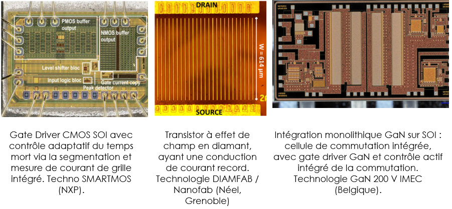
Achieving the highest performance in power converters requires mastery of emerging technologies such as CMOS microelectronic integration, GaN technologies, and ultra-wide bandgap materials (e.g., diamond). This research area aims to design and characterize new Gate Driver circuit architectures in CMOS technology for driving GaN and SiC transistors and modules, as well as to design the next generation of integrated functions and power components using GaN and diamond technologies.
Our group does not operate an in-house fabrication facility but has full access to state-of-the-art design, simulation, and manufacturing tools through our partnerships and expertise. This mastery enables us to develop functionalities that cannot be achieved through discrete component assemblies and to prototype the next generation of power switching components and cells.
Our expertise allows us to design these functions at the sub-micrometer and microampere scale and implement and demonstrate them in power switching cells operating at the macroscopic scale, handling several hundred amperes and hundreds of volts.
CMOS Gate Driver circuits for GaN and SiC power components:
Optimizing the switching behavior of wide bandgap transistors is a real challenge. High switching speeds reduce switching losses but generate electromagnetic interference (EMI) at high amplitudes and frequencies. We have proposed active switching control strategies, notably through feedback from the power stage to the control stage, in order to locally reduce the dV/dt during switching transients, improving the EMI/losses trade-off.
This is particularly challenging with medium-voltage GaN transistors, which can switch 400 V within a few nanoseconds. CMOS integration enables an analog bandwidth close to 10 GHz, making it possible—through optimization and analog amplification—to selectively reduce the gate current during the dV/dt phase via feedback control.
Thanks to the LabCom SEMA partnership, other integrated circuits using NXP’s SmartMOS technology have been developed to optimize and adaptively control the dead time of SiC switching cells or, in connection with Operation 4 of our group, to improve detection and protection against extreme short-circuit conditions.
Diamond power electronics, GaN monolithic integration, and beyond:
Wide bandgap devices such as SiC and GaN have been commercially available for many years, driving major breakthroughs in converter performance. However, ultra-wide bandgap materials like Ga₂O₃, h-BN, AlN, ZnOx, and diamond are identified as the next technological leap. Diamond is regarded as the ultimate material due to its unique properties.
This upstream activity is mainly driven by laboratories and start-ups with whom we closely collaborate (Institut Néel, DIAMFAB, University of Cambridge, University of Cádiz, Arizona State University, AIST). Our contributions have been recognized through our involvement in two European projects, one PEPR program (Frenchdiam), two ANR projects (including one coordination), and the “Etoiles de l’Europe” award for the GreenDiamond project, along with several other European project submissions during the period.
Through our close partnership with Institut Néel and the start-up DIAMFAB, significant advances have been made toward achieving the target of 1 kV and 1 A devices.
In addition, monolithic integration drastically reduces parasitic interconnections between the power components and their local control circuits. Lateral GaN technology enables such integration. We are currently designing and developing integrated control functions in GaN-on-SOI technology, through Europractice and IMEC technology (Belgium).

Electrical characterization bench for wide gap components in extreme operating conditions and associated close control integrated circuit.

Multiple original and impactful approaches: Innovative Gate-Driver Architectures, On-Chip Integration Technologies and In-Depth Multi-Physical Modeling of Failure Mechanisms
Largely focused on the research of fault-tolerant topologies until 2016–2017, this activity has since undergone significant thematic and foundational changes, returning to its roots by addressing topics broadly related to improving the reliability of wide-bandgap semiconductors, with a particular emphasis on their behavior under extreme fault conditions.
Indeed, the adoption of SiC MOSFET and GaN HEMT technologies remains very limited in critical and long-lifetime applications (e.g., railway and aerospace), mainly due to their inherently reduced and poorly understood reliability, as well as the highly demanding qualification requirements, particularly concerning short-circuit robustness.
To address this issue, our research aims, on the one hand, to propose innovative “compensation” solutions downstream, such as through gate-driver design (§4.1) and on-chip integration (§4.2); and on the other hand, upstream, to accurately characterize usage limits by implementing a comprehensive and in-depth multiphysics modeling approach of failure mechanisms under targeted and aggravated functional stress conditions (§4.3).
The most significant findings over the 2019–2024 period are presented below:
4.1 Multi-functional gate-driver architecture for real-time health monitoring of SIC MOSFET power chips and their short-circuit protection.
Our work has focused on a generic and multifunctional segmented-parallel gate driver architecture using selectively switched gate resistors. Two novel concepts have emerged specifically for SiC MOSFETs:
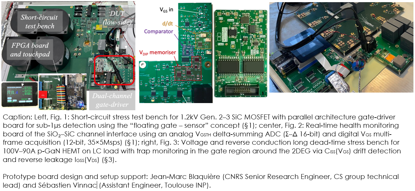
First, the “floating-sensing gate” between switching events, which offers high-sensitivity sub-microsecond detection of thermal gate leakage current under short-circuit type 1 conditions (natural Vgs depolarization with a fail-to-open ultimate failure mode), as well as detection of fault di/dt in type 2 conditions (natural Vgs overpolarization via Miller effect). Figure 1 shows the test bench where this first concept was validated, both with discrete components and high-current modules.
Second, the “ultra-slow triggering commutation” technique, which allows real-time, minimally intrusive extraction of multiple health indicators of the critical SiO2–SiC channel oxide interface. A dedicated approach for analog self-sampling of Vgs_th under low gate bias (a new method called the ‘Vgs dip’) and a generic high-resolution multi-frame digitization of Vgs were developed and compared using numerous experimental developments, as shown in Figure 2.
These two innovative techniques led to remarkable results in terms of precision and repeatability, with an accuracy margin of 0.5% on a 600V–20kHz PWM inverter (References: F. Boige’s PhD – collaborations with the Universities of Nottingham and Naples, 2019; M. Picot-Digoix, 2024; postdocs Y. Barazi – IRT Saint-Exupéry and W. Jouha, 2021; 4 patents, including 2 in TRL maturation in collaboration with Safran Tech; numerous awards).
Tara Niakan and Frédéric Richardeau – Electrical characterization bench for wide bandgap components in extreme operating conditions and associated close control integrated circuit.

4.2 Design and technological developments for ultimate integration with high reliability.
In close collaboration with Operation 3 of the CS group, the previously introduced concepts—particularly regarding short-circuit management—have been adapted and enhanced by leveraging ASIC CMOS integration of the gate driver. This approach provides significantly improved speed, precision, and immunity compared to the CMS integration discussed in §4.1.
Equally remarkable results have been achieved on high-current SiC MOSFET modules in 800V double-pulse tests, with protection delays of only a few hundred nanoseconds and high robustness against operating point variability (PhD thesis A. El Boubkari – 2024 – LabCom SEMA).
In a long-standing and close partnership with the ISGE team at LAAS, upstream work on vertical monolithic integration of switching cells is continuing, aiming to miniaturize and improve chip reliability by reducing the number of interconnections. This work has evolved toward multi-terminal SiC structures combining JBS diodes, VD-MOSFETs, and many new technological building blocks currently under study by L2n (lead institution) and LAAS. These include deep p+ implantation, semi-through isolation via high-energy etching, and buried metal vias for front-to-backside contact reconnection (ANR PRC MUS²-IC – 2022–2026 – coordinated and led by the CS group at Laplace).
4.3 Multi-physical modeling of failure mechanisms on targeted and aggravated functional stresses.
In direct connection with Operation 2 of the CS group, and from a more methodological perspective, building upon a strong foundation of experimental results and expertise developed in §4.1, a comprehensive (yet complex and demanding) multi-physics modeling approach using 2D Comsol™ was initiated in 2020 for a SiC MOSFET chip under short-circuit conditions.
The critical times and energy thresholds leading to the onset of source electrode melting and the cracking of the gate protection oxide can be extracted, allowing the specification of gate-driver protection time margins. This ensures that the chip can withstand repeated short-circuits without (significant) metallurgical and thermomechanical degradation (Postdoc by M. Shqair, 2023–2024, funded by the CS group’s internal resources, awarded 1st Prize at ESREF’23 Best Paper Awards, invited talk at IEEE IRPS’24 USA).
A similar modeling approach has been transposed to low-voltage GaN HEMTs, initiated in 2024 through an additional collaboration with the ISGE group at LAAS (ongoing PhD by Ms. N. Essobai), supported by experimental results from the PhD of L. Ghizzo (2022–2024).
Figure 3 shows one of the characterization test benches developed in partnership with Thales and CNES. New stress factors and associated degradation mechanisms have been identified in the p-GaN gate region and will soon be simulated using TCAD Sentaurus™, and then linked to Comsol™.
The Static Converters Group has design tools for prototype development as well as facilities for converter testing (4 × 15 kVA, 2 × 25 kVA, 1 × 60 kVA, 1 × 100 kVA, 150 kW grid connection and 50 kVA load), including control generation (digital, analog, HIL) and the design and characterization of CMOS integrated circuits used for both close and remote control of switching cells or power converters.
The Static Converters Group benefits from numerous industrial and academic partnerships:

Industrials: AIRBUS, ALSTOM and Transport Platform PRIMES, CIRTEM, HELION, LIEBBHER Aerospace, S2M, SCHNEIDER ELECTRIC-APC, SNCF-Engineering Department, NXP semiconductors, TECHNOFAN, RENAULT-TECHNOCENTRE, VALEO, ZODIAC, RONGXIN POWER ELECTRONIC Co, …
Academics : G2ELAB, LAAS ; SATIE, Insitut Néel, University of Cambridge, GRUCAS (Université Fédérale Santa Catarina, Brésil), LEEPCI (Université Laval, Quebec), Ecole Nationale d’Ingenieurs de Tunis – LSE, PowerLab (Université technique fédérale Santa Maria Valparaíso, Chili), IES, …
The CS group is the leader of the joint laboratory Embedded Systems for Autonomous Mobility SEMA, in partnership with the company NXP semiconductors and the LAPLACE and LAAS/CNRS laboratories (see SEMA web site)
The CS group is also the originator of numerous patents (freely accessible here), for example:
« MULTIPHASE DC TO DC CONVERTERS WITH PHASE SHEDDING, AND SUB-UNITS AND METHODS THEREFOR », Application Number 19306558.8 , NXP USA, Inc. and INSTITUT NATIONAL POLYTECHNIQUE DE TOULOUSE, date de dépôt 03 December 2019 , inventeurs : Loic HUREAU, Marc Michel COUSINEAU.
« DISTRIBUTED INTERLEAVING CONTROL OF MULTIPHASE SMPCS », Application Number 19306559.6 , NXP USA, Inc. and INSTITUT NATIONAL POLYTECHNIQUE DE TOULOUSE, date de dépôt 03 December 2019 , inventeurs : Miguel MANNES HILLESHEIM, Marc Michel COUSINEAU, Eric Pierre ROLLAND, Philippe GOYHENETCHE and Guillaume Jacques Leon AULAGNIER.
« DISTRIBUTED CONTROL OF A VOLTAGE REGULATOR », Application Number 19306578.6, NXP USA, Inc. and INSTITUT NATIONAL POLYTECHNIQUE DE TOULOUSE, date de dépôt 05 December 2019 , inventeurs : Guillaume Jacques Leon AULAGNIER, Miguel MANNES HILLESHEIM, Eric Pierre ROLLAND, Philippe GOYHENETCHE and Marc Michel COUSINEAU.
GATEAU, Guillaume, MEYNARD, Thierry, POSTIGLIONE, Gianluca, et al. Electric power converter. U.S. Patent Application No 16/420,128, 28 nov. 2019.“Multi-Level Inverter Topologies for Medium and High Voltage Applications,”
Odriozola, T.A. Meynard, and A. Lacarnoy, US patent A2000-7629 (APC-0704-US-PSP). (déposants Schneider Electric, CNRS, INPT)
« Détecteur de court-circuit pour transistor de puissance par surveillance du courant de sa grille », Frédéric RICHARDEAU, Jean-Marc BLAQUIERE, François BOIGE, Sébastien VINNAC, FR2011599, 12/11/2020, INSTITUT NATIONAL POLYTECHNIQUE DE TOULOUSE, CENTRE NATIONAL DE LA RECHERCHE SCIENTIFIQUE, UNIVERSITE TOULOUSE III – PAUL SABATIER
« MULTIPHASE DC TO DC CONVERTERS WITH PHASE SHEDDING, AND SUB-UNITS AND METHODS THEREFOR », Application Number 19306558.8 , NXP USA, Inc. and INSTITUT NATIONAL POLYTECHNIQUE DE TOULOUSE, date de dépôt 12/02/2020, inventeurs : Loic HUREAU, Marc Michel COUSINEAU.
« DISTRIBUTED INTERLEAVING CONTROL OF MULTIPHASE SMPCS », Application Number 19306559.6 , NXP USA, Inc. and INSTITUT NATIONAL POLYTECHNIQUE DE TOULOUSE, date de dépôt 12/02/2020, inventeurs : Miguel MANNES HILLESHEIM, Marc Michel COUSINEAU, Eric Pierre ROLLAND, Philippe GOYHENETCHE and Guillaume Jacques Leon AULAGNIER.
« DISTRIBUTED CONTROL OF A VOLTAGE REGULATOR », Application Number 19306578.6, NXP USA, Inc. and INSTITUT NATIONAL POLYTECHNIQUE DE TOULOUSE, date de dépôt 12/02/2020, inventeurs : Guillaume Jacques Leon AULAGNIER, Miguel MANNES HILLESHEIM, Eric Pierre ROLLAND, Philippe GOYHENETCHE and Marc Michel COUSINEAU.
« MODULAR INTERLEAVING TECHNIQUES FOR SCALABLE POWER ELECTRONICS CONVERTER », Application Number 20305395.4, NXP USA, Inc. and INSTITUT NATIONAL POLYTECHNIQUE DE TOULOUSE, date de dépôt 12/02/2020, inventeurs : Miguel MANNES HILLESHEIM, Marc Michel COUSINEAU, Eric Pierre ROLLAND, Philippe GOYHENETCHE and Guillaume Jacques Leon AULAGNIER.
FR 252156 – « PROCEDE DE COMMANDE D’UN CONVERTISSEUR ALTERNATIF-CONTINU DE TYPE MMC, CONVERTISSEUR ALTERNATIF CONTINU DE TYPE MMC ET PRODUIT PROGRAMME D’ORDINATEUR », D. GUEDON, S. CORNET, P. LADOUX, S. SANCHEZ – Co-déposants EDF, CNRS, INPT – Décembre 2020.
Multi-level inverter topologies for medium-and high-voltage applications ; K Odriozola, T Meynard, A Lacarnoy ; US Patent App. 16/883,174
Electric power converter, G Gateau, T Meynard, G Postiglione, G Borghetti, D Falchi, US Patent 10,574,130
Luc BIMMEL soutiendra sa thèse le vendredi 20 février 2026 à 09 h 00 en salle des thèses de l’ENSEEIHT (Amphi C002), au 2 Rue
Daniel GALVIS soutiendra sa thèse le mardi 03 février 2026 à 14 h 00 – salle de thèses C002 à l’ENSEEIHT, sur le sujet : «
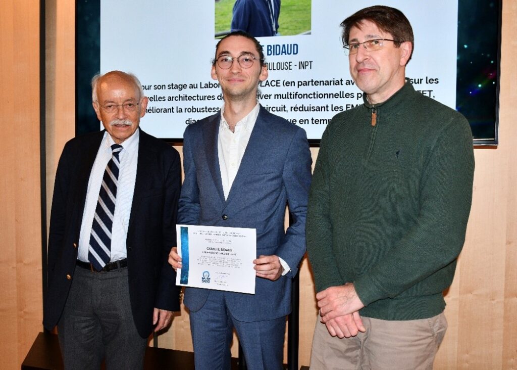
Les travaux de PFE Ingénieur ENSEEIHT et de Master Recherche de Camille Bidaud viennent d’être honorés successivement par le 1er Prix “Jeunes” de la SEE
Joseph Kemdeng soutiendra sa thèse le mercredi 17 décembre 2025 à 09h30 – Salle des thèses ENSEEIHT (C002), sur le sujet : Intégration monolithique d’un
Thomas DIAS soutiendra sa thèse le jeudi 20 novembre 2025 à 9h30 – Salle des thèses, ENSEEIHT, sur le sujet : Convertisseur pour station de recharge
Mathis Picot-Digoix soutiendra sa thèse Cifre le vendredi 3 octobre 2025 à 13h30, site de l’ENSEEIHT, salle C002, sur le sujet : Architectures multi-niveaux et
Le 6ème symposium de génie électrique, SGE2025, a eu lieu à Toulouse du 1er au 3 Juillet, au centre de congrès Pierre Baudis. Ce symposium,
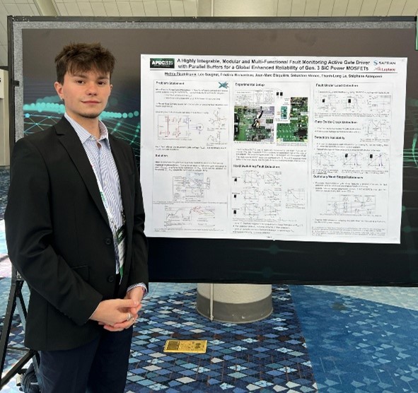
Mathis Picot-Digoix à la Session d’ouverture Preview Highlight Poster de l’IEEE Applied Power Electronics Conference and Exposition (APEC), le 17 mars 2025 à Atlanta, USA.
La soutenance de thèse de Damien MICHEZ intitulée : “Fabrication et caractérisation de transistor à effet de champ en diamant en vue de l’augmentation du